Rolls of sheet metal
PCBs
Semiconductor wafers
Thin film on a roll in an industrial setting

Accurate and Efficient Evaluation of the Full Film or Coating with High Spatial Resolution

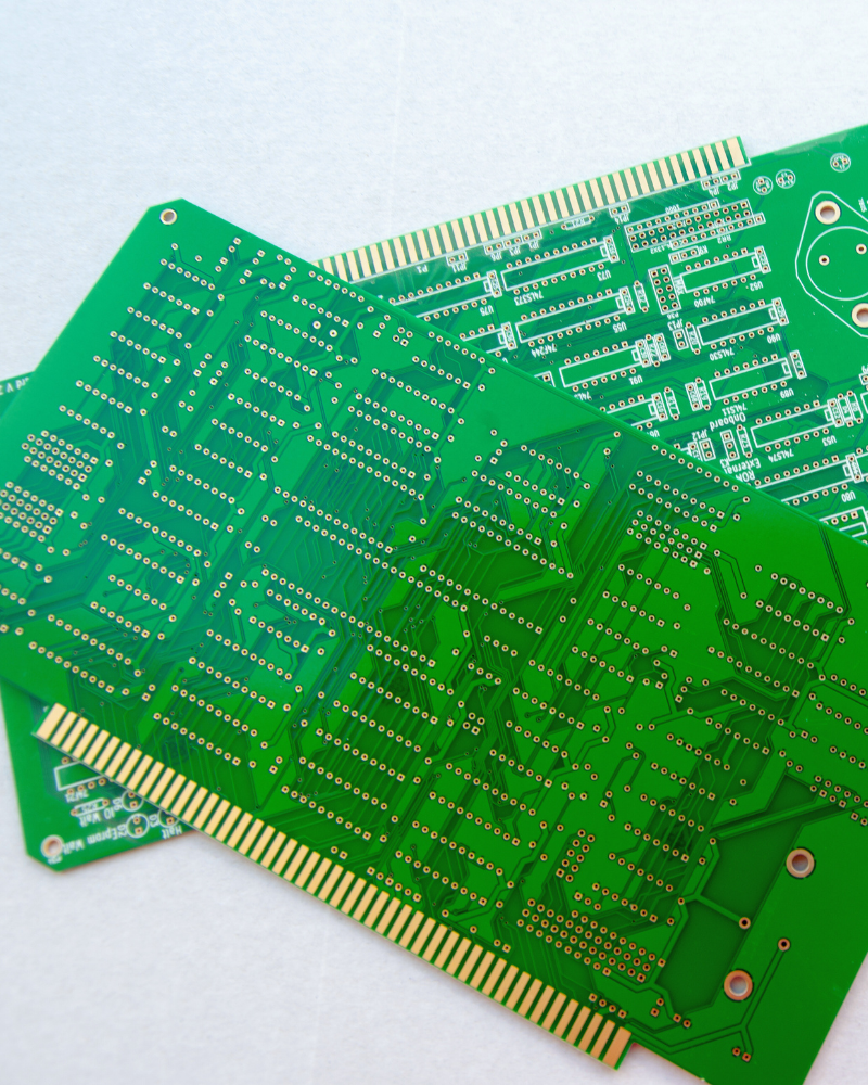
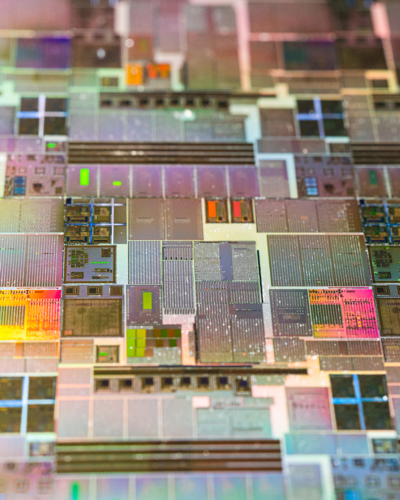
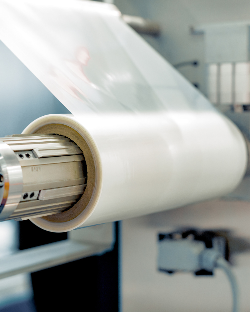
Coatings play a critical role in determining a product’s quality, functionality, and long-term durability across a wide range of industries.

The condition of a surface often provides valuable insight into structural integrity, performance, and visual appearance. Even minor coating defects, material impurities, or application inconsistencies can compromise reliability, reduce lifespan, or introduce safety risks, making thorough surface inspection an essential part of quality assurance.

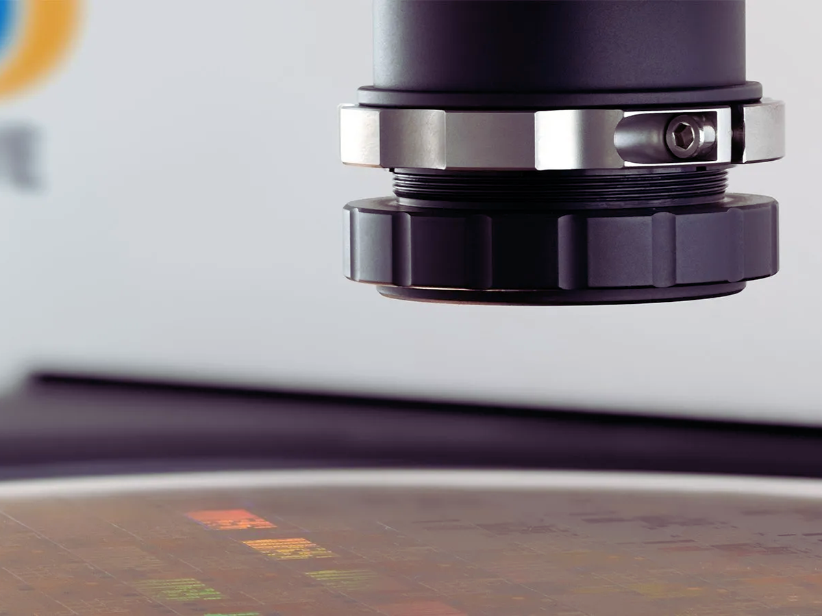
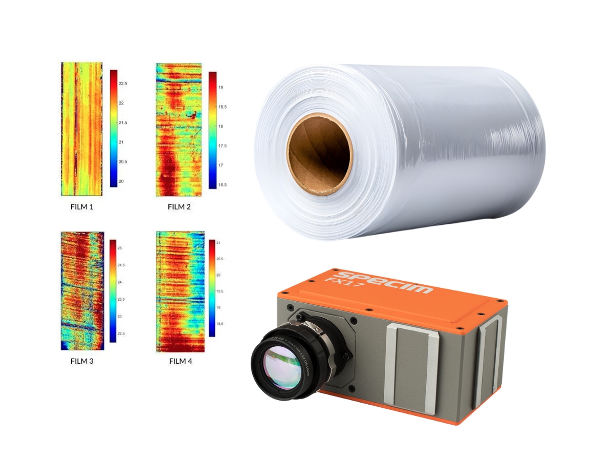
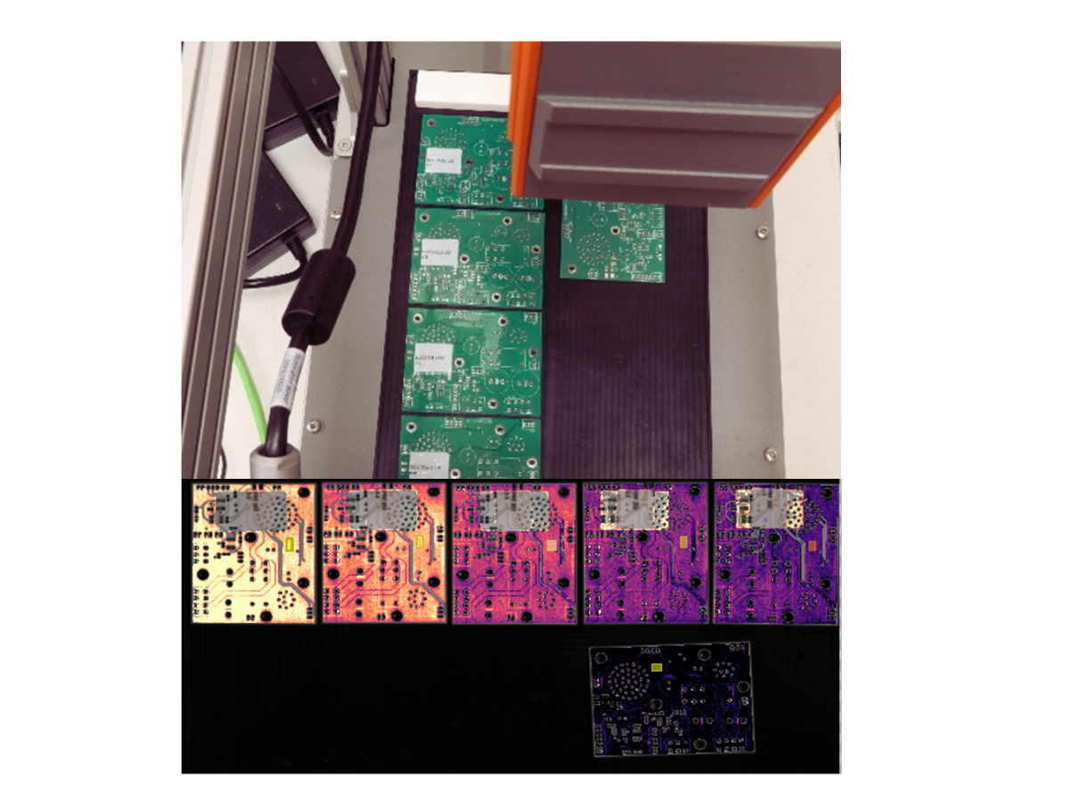
Hyperspectral imaging delivers a highly accurate, non-destructive, and contact-free approach to surface and coating inspection in real time. Rather than relying on traditional point-based measurements, hyperspectral imaging technology captures complete spatial and spectral information across the entire surface, ensuring comprehensive coverage and analysis. 

Hyperspectral data enables precise evaluation of coating layer thickness, early detection of subtle surface defects or contaminants invisible to standard imaging, and detailed assessment of coating homogeneity and uniformity. The result is greater confidence in coating quality, improved process control, and more consistent product performance.

Hyperspectral camera above semiconductor wafers inspecting during production

Key Benefits of Hyperspectral Imaging for Surface Coating & Inspection:

  • Contact-Free & Non-Destructive: Analyze coatings and surfaces without damaging the product or interrupting production.
  • Insights in Real-Time: In-line monitoring for immediate quality control and process optimization.
  • Complete Surface Coverage: Inspect entire surfaces rather than single points, ensuring no defects or inconsistencies are missed.
  • Early Detection of Subtle Defects: Identify micro-defects, impurities, and material variations that are invisible to the human eye or conventional imaging.
  • Material and Chemical Differentiation: Distinguish between different coating materials, contaminants, or substrate variations based on spectral signatures.
Plastic film roll beside spectral thickness map and FX17 camera

Thin Film Inspection

Thickness and homogeneity significantly impact functionality of thin films and coatings, and are critical quality parameters to monitor during production. 

Hyperspectral imaging offers the ability to evaluate many parameters during the production of thin films, including layer presence, thickness, material, roughness and porosity. Hyperspectral cameras, such as the Specim FX17, can be used to quickly and efficiently detect contamination, residue and debris, as well as defects, cracks and holes.

Hyperspectral imaging offers a significant advantage over point spectrometers in this application as it allows for inspection of the full film or coating as opposed to individual point samples, resulting in spectroscopic data across the full width at high spatial resolution.


Application Note: Thin Film Thickness Inspection by Hyperspectral Imaging

PCBs on the Specim LabScanner beside a spectral image showing differences in surface coating

PCB Quality Inspection

NIR hyperspectral imaging solutions, such as the Specim FX17, offer a powerful, non‑destructive way to assess printed circuit board (PCB) quality by capturing detailed spectral data across each pixel of an image. 

Unlike traditional visual or fluorescence methods that only reveal where a coating is present, hyperspectral systems measure how materials interact with light across a broad range of wavelengths, particularly in the near‑infrared. This makes it possible to not only detect different types of protective coatings applied to PCBs but also to quantify their thickness and uniformity with high precision. 

Incorporating hyperspectral imaging into PCB inspection workflows significantly enhances quality control by delivering full‑surface coverage and detailed material characterization. Because every pixel contains spectral information, defects or inconsistencies that might be missed by conventional imaging can be identified early in the manufacturing process. 

This capability is especially valuable for ensuring that protective coatings meet specified thickness ranges and are applied evenly, factors that strongly influence PCB longevity and performance. By automating inspection and providing quantitative data on coating properties, hyperspectral systems help manufacturers maintain higher reliability standards across a wide array of electronic products.


Application Note: Enhancing PCB Quality Inspection with Hyperspectral Imaging

Sheet Metal on rollers

Surface Inspection in the Metal Industry

Ensuring the quality and integrity of metal surfaces, particularly hot steel, is a critical challenge in manufacturing environments such as rolling mills and press shops. 

Hyperspectral imaging provides a highly precise, non-contact method for inspecting surface coatings, including oil, water, wax, lacquer, and other protective chemicals, while also detecting impurities, defects, and contamination. 

By accurately measuring coating thickness from nanometers to micrometers, this technology enables early identification of inconsistencies and potential material issues, supporting superior quality control and consistent product performance.